A Light Design
Welcome back to this blog series about making a set of programmable party lights. In the previous post, I outlined the background and general plan for the project. Now we’re getting to the interesting bit: the first board design!
This board (as is every board I make) was designed in KiCad. I’m a great advocate of the Open Source movement and I try to use open source tools whenever possible. I’ve been using KiCad since version five. As I write this they’re at version eight and the software amazes me with every new release. If you’re not familiar with the project, go check it out! If you like it and have some money to spare, you might want to consider donating to the project.
Another project that deserves some love is the KiCanvas project by Thea Flowers. KiCanvas is the plug-in that shows the KiCad designs below.
Laying Block
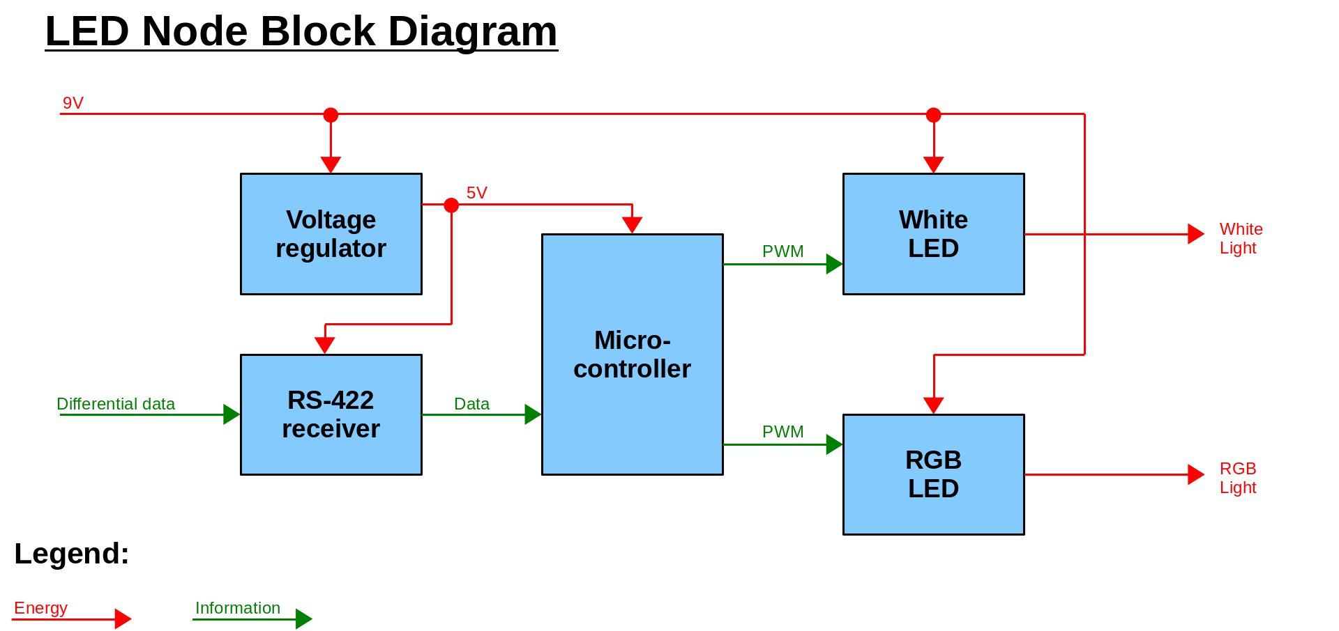
A nice block diagram is always a good starting point for any design. So here goes.
 Blocks again
The LED board design is actually pretty straightforward. The microcontroller gets its information from the controller board via the serial receiver and interprets the protocol. It then sends out a PWM signal to control the LEDs. The power supply converts the 9 Volts supply voltage to 5 Volts for the control logic, while the LEDs are powered directly from the power rail and switched using low side BJTs.
Being Cheap
When building just a few boards, costs aren’t that big of an issue. But when the number of units grows, even to a dozen or two, the costs start adding up quickly. It pays to keep the unit price of the components in mind. The same goes for the bare board. There’s never a free lunch, so some compromises will have to be made to keep the costs within bounds.
I’ll discus the main components below.
Microcontroller
The most critical part, at least when it comes to silicon, will be the microcontroller. We need the basic peripherals like a UART, and PWM generators. We also need a spare timer for protocol decoding and ideally a timer to track idle time so we can put the LED nodes in a low power mode when they’re not being used. I like to work with Microchips Attiny series of microcontrollers whenever I need a simple controller at an acceptable price point. Their AVR0 series seem just about perfect for this job. I picked the Attiny4021, which came at about 0.40 Euros at the time I worked on the project.
The nice people of the Microchip marketing department point out the following features:
- Two general purpose timers with PWM
- One Real Time Clock (RTC)
- A UART
- A built-in oscillator
Just the thing I need! No real compromises here.
LEDs
I found it rather hard to estimate the right type and number of LEDs to achieve sufficient brightness. Too little light output would make the set rather useless. There is also a constraint on the total current consumption as all the LEDs current will be carried trough three conductor pairs in the UTP cable. UTP being a data cable, the conductors are small in diameter. The conduction losses will go up quickly, even with just one white LED and one RGB LED on each of the 25 nodes.
With the project having a clear deadline, there was no time to do extensive testing. So I ended up picking some reasonably priced parts with forward currents that weren’t too high and hoped for the best.
For the downlights I choose two, 5mm through hole LEDs from Everlight (part no. 334-15/X2C1-1WYB2). They will be mounted at the edge of the board at a 90 degree angle, pointing downwards. There will be two in series, making the combined forward voltage 8.2 volts. The datasheet doesn’t mention the nominal forward current, but based on experience I estimated that 50mA would be a reasonable guess.
The RGB LEDs are surface mount parts. The IN-P55TATRGB3 by Innolux are rather large LEDs with a big circular optical area. They draw 20mA per channel at 2.4, or 3.1 volts, depending on the color. Just like the white LEDs there will be two in series. One each side of the board.
Power Supply
This is where compromises had to be made. The LEDs will be powered from a 9 Volts power rail. The logic runs on 5 Volts. A switch mode power supply would be too expensive and add too many parts to the board. I opted for a linear regulator instead. Low cost and low part count, but also low efficiency. Not all linear regulators are created equal. True, they all dissipate the excess power as heat, hence the inefficiency. But even inefficiency comes in grades. The regulator will need some power to run, i.e. its quiescent current. And low quiescent current doesn’t come cheap. If one were to draw a Venn diagram of efficiency versus price point, it will look something like this:
 No free lunch
I picked a part from the left hand side circle, namely the UA78L05ACDR4 (Texas Instruments). In hind sight however, this may not have been the best decision. The 7805 family aren’t famous for their high efficiency and the UA78L05ACDR sip about 6mA while doing nothing at all. This quickly adds up with 25 boards. Not necessarily a good thing for a battery powered device.
Receiver
This brings us to the reason for exchanging power efficiency for price point: the RS-422 transceiver. This chip costs as much as the voltage regulator and microcontroller combined. This begs the question: why use it in the first place?
For smooth light effects the RGB LEDs will have to be updated at a rate of approximately 25 frames per second. There are 25 nodes with 4 LEDs. With 8 data bits, a start bit and a stop bit, that will add up to 25 kbits per second. And that’s the bare minimum. Ideally the transfer speed would be much higher. This data will have to travel approximately 10 meters, passing multiple circuit boards, solder joints and vias. Transferring data over a single ended link comes with some challenges. Sure, it can be done, but it will take extra time to make the data link reliable as the cables will pick up noise and deteriorate the signal. The receiving ends will need filtering, which limits the overall speed, and ideally the communication protocol would need some form of error detection. That will also add to the development time and firmware overhead. So, on the whole I thought it wiser to go for a fail safe solution and use differential signaling in the form of RS-422. This eliminates pickup by the cables and allows for high data speeds. The latter allows the design to be used for a larger number of nodes where more data will have to be sent for a single frame.
The RS-422 receiver chosen is the THVD1500D5 by Texas Instruments. It comes at 80 cents.
Pulse Width Modulation… Sort of.
The Attiny 402 comes with two general purpose timers that can generate four independent PWM waveforms. Three of the PWM generators are part of Timer/Counter A, the fourth is part of Timer/Counter B. The PWM outputs share the GPIO pins with other peripherals.
I will be needing one Timer/Counter peripheral for protocol decoding. That will be Timer/Counter B as that can only drive one PWM output. That leaves Timer/Counter A to control the LEDs. There are four waveform generator outputs linked to this Timer/Counter. The problem is that one of them shares a pin with the UART receiver. It so happens that the LED boards will need to get their data from that precise pin. So if we want both PWM and a serial receiver we’d have to implement one of them in firmware, bypassing the peripherals. This would be highly resource-intensive, not to mention add a significant amount of firmware to the already limited flash space. So we can’t have a both. Or can we?
In fact, we can! But it takes a hack to do so. Pulse width modulation is in essence just a square wave of which the on to off ratio changes. The average output power matches this ratio.
Now lets have look a the common UART protocol. This too, is essentially a square wave. A power source that bounces between 0% and 100% output power. The default state of a UART peripheral is logic high (i.e. 100% power). To initiate the transmission the line goes low for one bit time (the start bit). Then follow a number of data bits (either 0% or 100% power), then a stop bit that’s always low (0%). The graph below compares a UART sending seven high bits and one low bit to a pulse width modulation of 80%.
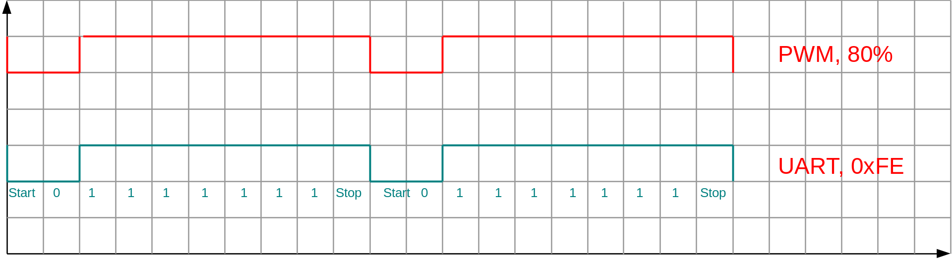 UART pretending to be PWM
Both waveforms have an on to off ratio of 80%, meaning that the UART can mimic a PWM generator. The solution isn’t perfect though. For one, we don’t have a full 0 - 100% modulation range at our disposal due to the mandatory start and stop bits. The dimming resolution is also very limited as we can’t transmit fractions of bits. This can be addressed in part by sending out patterns of more than one byte. That will however lower the effective frequency of the waveform and there will be a point where it gets low enough for the human eye to perceive (and thus become annoying).
Why is this a solution the problem? The protocol to control the LEDs will be one way traffic. This means we will only need the receive pin for the data and can hack the transmitter to modulate one of the LEDs. We now have Timer/Counter B available for various timing tasks in the firmware.
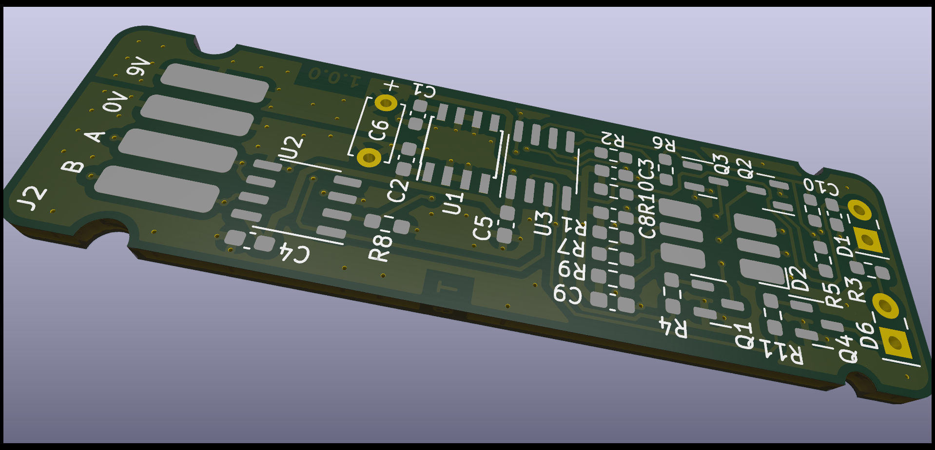
Schematic Design
You’ll find the schematic of the controller board below. Or you can view a pdf if the KiCanvas viewer doesn’t work in your browser.
After the lengthy discussion of the components there’s really not too much to say about the schematic as the design is actually quite straightforward.
- Data and power enter via connector J1. J2 allows the nodes to be daisy chained. The connectors are actually solder pads as the wiring will be soldered directly to the board.
- U1 provides 5 Volts to the controller and transceiver.
- U2 is the RS-422 transceiver chip. The Driver Enable input is permanently pulled to ground as only the receiver will be used.
- The microcontroller, U3, controls the transistors that enable the LEDs. R2 is an extra (weak) pull-up for the reset pin that is not strictly needed as it is pulled up internally. A bypass capacitor should probably be better instead, although the datasheet does not make any specific recommendation in that regard.
- The resistors in series with the LEDs limit their current to make them work on 9 Volts. I used 0603 surface mount parts and had to put two in series with the red LEDs as their forward voltage is lower. This means higher dissipation in the resistors.
- Capacitors C3, C8, C9 and C10 bypass any high frequency noise generated by the fast edges of the PWM signal. They can probably be omitted but I consider it good practice to bypass fast switching loads.
- Electrolytic capacitor C6 acts as a bulk capacitor to keep the voltage steady for the LEDs.
There are also some test points and two mystery resistors: R8 and the oddly named R101. All of these are for the board to be used in a jig for programming and testing. The test jig will come with pogo pins that connect to these test points.
- The 9V pad of J1 will provide power to the board, just as in normal operation.
- TP1 is the ground reference.
- TP2 is to measure the 5V rail to verify proper operation of the voltage regulator.
- TP4, TP5 and TP7 are for an optional factory mode.
The idea behind the factory mode was that the microcontroller would sample the state of pin PA3 at start-up. In case of the board being in the test jig this pin would be pulled high via TP7. In normal operation R101 would keep it at a low logic state. TP4 would also be pulled high by the jig, putting the data output of the receiver (U2) in high impedance mode. This way a USB to serial converter (or another microcontroller) would interface directly with the microcontroller.
Would. Because, unfortunately, there was no more flash memory to spare and the function couldn’t be implemented. At least you now know what the extra parts are for.
Board Layout
The glass jars that will become the home of these boards aren’t very large. They have a 20mm diameter hole at the top and are about 77mm deep. The boards will be pointing downwards and the 5mm LEDs will be protruding from the board edge. At the mouth of the jar some space will have to be reserved for the cable, a strain relief and a mounting mechanism for the board. The boards are 17mm wide and 57mm tall.
The board will snap into a mounting mechanism. A notch will fall into the cut-outs at the side of the board, near the cable entry. More on that in a future post. There’s also cut-out at the other end of the board, near the LEDs. That will hold a 3D printed diffuser in place that will cover the RGB LEDs (as well as most of the board).
As there aren’t many signal and power traces needed in this design, a two layer board will do. The bottom layer is primarily the ground plane but for one LED and the test points.
Design Files
The board design is available on my Gitlab repository. It is licensed under the CERN-OHL-S license, which is included in the repository).
The next article will cover building the board.